- 您现在的位置:买卖IC网 > Sheet目录287 > 24LC1025-E/P (Microchip Technology)IC EEPROM 1MBIT 400KHZ 8DIP
�� �
�
�24AA1025/24LC1025/24FC1025�
�2.0�
�PIN� DESCRIPTIONS�
�The� descriptions� of� the� pins� are� listed� in� Table� 2-1� .�
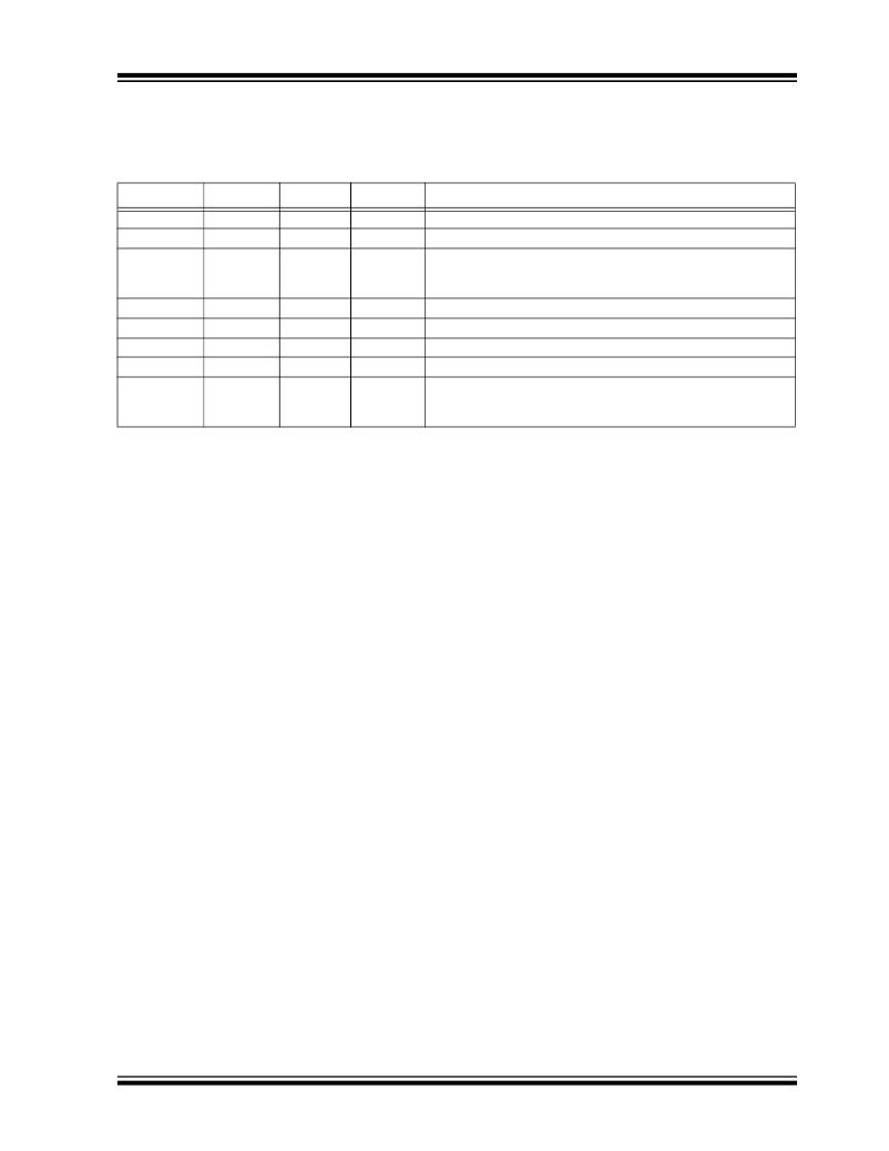
�TABLE� 2-1:�
�PIN� FUNCTION� TABLE�
�Name�
�A0�
�A1�
�A2�
�PDIP�
�1�
�2�
�3�
�SOIJ�
�1�
�2�
�3�
�SOIC�
�1�
�2�
�3�
�Function�
�User� Configurable� Chip� Select�
�User� Configurable� Chip� Select�
�Non-Configurable� Chip� Select.�
�This� pin� must� be� hard-wired� to� logical� 1� state� (V� CC� ).� Operation� will�
�be� undefined� with� this� pin� left� floating� or� held� to� logical� 0� (V� SS� ).�
�V� SS�
�SDA�
�SCL�
�WP�
�V� CC�
�4�
�5�
�6�
�7�
�8�
�4�
�5�
�6�
�7�
�8�
�4�
�5�
�6�
�7�
�8�
�Ground�
�Serial� Data�
�Serial� Clock�
�Write-Protect� Input�
�+1.7� to� 5.5V� (24AA1025)�
�+2.5� to� 5.5V� (24LC1025)�
�+1.8� to� 5.5V� (24FC1025)�
�2.1�
�A0,� A1� Chip� Address� Inputs�
�2.3�
�Serial� Data� (SDA)�
�The� A0� and� A1� inputs� are� used� by� the� 24XX1025� for�
�multiple� device� operations.� The� levels� on� these� inputs�
�are� compared� with� the� corresponding� bits� in� the� slave�
�address.� The� chip� is� selected� if� the� comparison� is� true.�
�Up� to� four� devices� may� be� connected� to� the� same� bus�
�by� using� different� Chip� Select� bit� combinations.� In� most�
�applications,� the� chip� address� inputs� A0� and� A1� are�
�hard-wired� to� logic� ‘� 0� ’� or� logic� ‘� 1� ’.� For� applications� in�
�which� these� pins� are� controlled� by� a� microcontroller� or�
�This� is� a� bidirectional� pin� used� to� transfer� addresses�
�and� data� into� and� data� out� of� the� device.� It� is� an� open-�
�drain� terminal,� therefore,� the� SDA� bus� requires� a� pull-�
�up� resistor� to� V� CC� (typical� 10� k� ?� for� 100� kHz,� 2� k� ??� for�
�400� kHz� and� 1� MHz).�
�For� normal� data� transfer� SDA� is� allowed� to� change� only�
�during� SCL� low.� Changes� during� SCL� high� are�
�reserved� for� indicating� the� Start� and� Stop� conditions.�
�other� programmable� device,� the� chip� address� pins�
�must� be� driven� to� logic� ‘� 0� ’� or� logic� ‘� 1� ’� before� normal�
�2.4�
�Serial� Clock� (SCL)�
�device� operation� can� proceed.�
�This� input� is� used� to� synchronize� the� data� transfer� from�
�and� to� the� device.�
�2.2�
�A2� Chip� Address� Input�
�2.5�
�Write-Protect� (WP)�
�The� A2� input� is� non-configurable� Chip� Select.� This� pin�
�must� be� tied� to� V� CC� in� order� for� this� device� to� operate.�
�If� left� floating� or� tied� to� V� SS� ,� device� operation� will� be�
�undefined.�
�?� 2005-2012� Microchip� Technology� Inc.�
�This� pin� must� be� connected� to� either� V� SS� or� V� CC� .� If� tied�
�to� V� SS� ,� write� operations� are� enabled.� If� tied� to� V� CC� ,�
�write� operations� are� inhibited,� but� read� operations� are�
�not� affected.�
�DS21941K-page� 5�
�发布紧急采购,3分钟左右您将得到回复。
相关PDF资料
24LC16BH-E/P
IC EEPROM 16KBIT 400KHZ 8DIP
24LC21-I/P
IC EEPROM 1KBIT 400KHZ 8DIP
24LC21A/P
IC EEPROM 1KBIT 400KHZ 8DIP
24LC22A-I/P
IC EEPROM 2KBIT 400KHZ 8DIP
24LC64XT-I/ST
IC SERIAL EEPROM 64K 2.5V 8TSSOP
24LCS21A/P
IC EEPROM 1KBIT 400KHZ 8DIP
24LCS22A-I/P
IC EEPROM 2KBIT 400KHZ 8DIP
24VL014/SN
IC EEPROM 1KBIT 400KHZ 8SOIC
相关代理商/技术参数
24LC1025-E/SM
功能描述:电可擦除可编程只读存储器 1024K 128KX8 2.5V SER EE 128 BYTE PAGE RoHS:否 制造商:Atmel 存储容量:2 Kbit 组织:256 B x 8 数据保留:100 yr 最大时钟频率:1000 KHz 最大工作电流:6 uA 工作电源电压:1.7 V to 5.5 V 最大工作温度:+ 85 C 安装风格:SMD/SMT 封装 / 箱体:SOIC-8
24LC1025-E/SN
功能描述:电可擦除可编程只读存储器 1024K 128K X 8 2.5V RoHS:否 制造商:Atmel 存储容量:2 Kbit 组织:256 B x 8 数据保留:100 yr 最大时钟频率:1000 KHz 最大工作电流:6 uA 工作电源电压:1.7 V to 5.5 V 最大工作温度:+ 85 C 安装风格:SMD/SMT 封装 / 箱体:SOIC-8
24LC1025-I/P
功能描述:电可擦除可编程只读存储器 1024K 128KX8 2.5V SER EE RoHS:否 制造商:Atmel 存储容量:2 Kbit 组织:256 B x 8 数据保留:100 yr 最大时钟频率:1000 KHz 最大工作电流:6 uA 工作电源电压:1.7 V to 5.5 V 最大工作温度:+ 85 C 安装风格:SMD/SMT 封装 / 箱体:SOIC-8
24LC1025-I/P
制造商:Microchip Technology Inc 功能描述:EEPROM IC Leaded Process Compatible:Yes
24LC1025-I/SM
功能描述:电可擦除可编程只读存储器 1024K 128KX8 2.5V SER EE RoHS:否 制造商:Atmel 存储容量:2 Kbit 组织:256 B x 8 数据保留:100 yr 最大时钟频率:1000 KHz 最大工作电流:6 uA 工作电源电压:1.7 V to 5.5 V 最大工作温度:+ 85 C 安装风格:SMD/SMT 封装 / 箱体:SOIC-8
24LC1025-I/SN
功能描述:电可擦除可编程只读存储器 1024K 128K X 8 2.5V RoHS:否 制造商:Atmel 存储容量:2 Kbit 组织:256 B x 8 数据保留:100 yr 最大时钟频率:1000 KHz 最大工作电流:6 uA 工作电源电压:1.7 V to 5.5 V 最大工作温度:+ 85 C 安装风格:SMD/SMT 封装 / 箱体:SOIC-8
24LC1025-IP
制造商:MICROCHIP 制造商全称:Microchip Technology 功能描述:1024K I2Ca?¢ Serial EEPROM
24LC1025-I-SM
制造商:MICROCHIP 制造商全称:Microchip Technology 功能描述:1024K I2Ca?¢ Serial EEPROM